Automated e-Beam
Workflow to contact randomly oriented micro structures - VIDEO
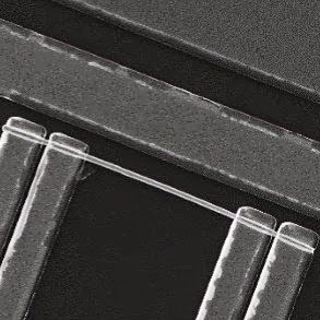
In the external page Laboratory of Semiconductor Materials of Prof. Fontcuberta i Morral at EPFL, PhD candidate Daniel Rüffer and former group member Dr. Martin Heiss have developed a workflow to automate the contacting of randomly positioned micron-sized structures.
Key feature of this workflow is a python-based pattern-recognition software. From pictures taken with an optical microscope, the software generates a script that will guide an e-beam machine to contact a large number of random microstructures. To that end, the microstructures are distributed on pre-patterned wafers. The pattern shapes and structures are optimized such that the software can determine the position of the samples as accurate as 100 nm.